WE MAKE THE MOST OF DIGITAL AND RF TECHNOLOGIES

RF Module 3 ports - 4 components

Diagrams mechanics / 3d and case

J1: Input / J2: Input / J3: Output

Description

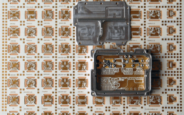
Pick your choice from our circuit’s library cells to make your design. We check it, build it and verify its specifications. As a result: a multi integrated functions module tailored to your needs at very low added cost.
Synopsis Technologies has developed a low cost versatile set of solutions in order to obtain many microwaves (up to 20GHz) solutions in a few weeks.
It is based on standard multilayer PCBs receiving the bias circuit and some simple control circuits (often to offset the control signal from a TTL input level to a 0/-5V control signal).A USB interface module is also available to help you control the digitally controlled cells through this interface

Exemple of Module RF synopsis


Library of RF label

Couplers

Reference Pin Arragement Function name Frequence Min (GHz) Frequence Max (GHz) Direct Gain (dB) Coupling (dB) Isolation (dB) NF (dB) P1db (dBm) OIP3 (dBm) VSWR In VSWR Out
CF15R5-L1
Coupler 7 14 -1,5 17 10 NA NA 1,8 1,8
CF15R5-L2
Coupler 7 14 -1,5 17 10 NA NA 1,8 1,8
CF15R5-L3
Coupler 7 14 -1,5 17 10 NA NA 1,8 1,8

Amplifiers

Reference Pin Arragement Function name Frequence Min (GHz) Frequence Max (GHz) Direct Gain (dB) Coupling (dB) Isolation (dB) NF (dB) P1db (dBm) OIP3 (dBm) VSWR In VSWR Out
AMP-XX
SOT89 Amplifiers 0,1 8 up to 20 NA 20 from 1.5 up to 21 up to 44 2 2
LNA-1
Low Noise Amplifiers 5 10 18,5 NA 25 2 16 28 2 2
LNA-2
Low Noise Amplifiers 6 17 17 NA 25 2,3 12,5 25 2 2
LNA-3
Low Noise Amplifiers 0,1 20 11 NA 25 4 14 28 2 2
LNA-4
Low Noise Amplifiers 2 18 15 NA 25 4 13 24 2,3 2
LNA-5
Low Noise Amplifiers 5 18 11 NA 25 6,5 17 25 2 2
MPA-1
Medium Power Amplifier 0,1 20 12 NA 25 5 24 35 2 2
PA-1
Power Amplifier 0,1 18 10 NA 25 5 24 35 2 2
PSA-1
Splitted Amplifier 7 14 6 NA 25 6,5 11 19 2 2

Attenuators

Reference Pin Arragement Function name Frequence Min (GHz) Frequence Max (GHz) Direct Gain (dB) Coupling (dB) Isolation (dB) NF (dB) P1db (dBm) OIP3 (dBm) Range VSWR In VSWR Out
SA-1
Step Attenuator 0,1 18 -7 NA -7 7 25 43 5 bit 31dB 2 2
PAD-1
Fixed Attenuator DC 18 0 to 30 NA NA NA NA 1,7 1,9

SPDT / SPST

Reference Pin Arragement Function name Frequence Min (GHz) Frequence Max (GHz) Direct Gain (dB) Coupling (dB) Isolation (dB) NF (dB) P1db (dBm) OIP3 (dBm) VSWR In VSWR Out
SPDT-1
SPDT non reflective 0,1 18 -3 NA 30 3 23 45 2 2
SPDT-2
SPDT non reflective 0,1 18 -3 NA 30 3 23 45 2 2
SPDT-3
SPDT 0,1 18 -2 NA 35 2 30 48 2 2
SPDT-4
SPDT 0,1 18 -2 NA 35 2 30 48 2 2
SPST-1
SPST 0,1 18 -2 NA 35 2 30 48 2 2

Multipliers

Reference Pin Arragement Function name Frequence Min (GHz) Frequence Max (GHz) Direct Gain (dB) Coupling (dB) Isolation (dB) NF (dB) P1db (dBm) OIP3 (dBm) VSWR In VSWR Out
X2-1
Multiplier x2 1,2 4,4 -15 NA NA NA NA NA
X2-2
Multiplier x2 2,6 7,2 -15 NA NA NA NA NA
X2-3
Multiplier x2 5 10 -15 NA NA NA NA NA
X2-4
Multiplier x2 10 20 -15 NA NA NA NA NA
X2-5
Multiplier x3 3 4,5 -15 NA NA NA NA NA

Mixers

Reference Pin Arragement Function name Frequence Min (GHz) Frequence Max (GHz) Direct Gain (dB) Coupling (dB) Isolation (dB) NF (dB) P1db (dBm) OIP3 (dBm) VSWR In VSWR Out
MIX-1
Mixer 6 12 -9 NA 25 10 19 30 2,3 2
MIX-2
Mixer 6 18 -11 NA 30 11 16 18 2,3 2,3
MIX-3
Mixer with optional maching pad 6 18 TDB NA TDB TDB TDB TDB 2 2
MIX-4
Mixer 6 18 -11 NA 30 11 10 18 2,3 2,3
MIX-5
Mixer 3 10 -10 NA 30 10 15 23 3 3
MIX-6
Mixer with optional matching pad 3 10 TDB NA TDB TDB TDB TDB 2 2
MIX-7
Mixer 3 10 -10 NA 30 10 15 23 3 3
MIX-8
Mixer 1 18 -9 NA 20 9 15 25 2,7 2

LPF / BPF

Reference Pin Arragement Function name Frequence Min (GHz) Frequence Max (GHz) Direct Gain (dB) Coupling (dB) Isolation (dB) NF (dB) P1db (dBm) OIP3 (dBm) Range VSWR In VSWR Out
LPF-L1-XX
LPF cutoff 0,1 cutoff 12 0 to -3 NA 20 at cutoff 1,2 NA NA NA 1,8 1,8
LPF-L2-XX
LPF cutoff 0,1 cutoff 7,2 0 to -3 NA 20 at cutoff 1,2 NA NA NA 1,8 1,8
LPF-L3-XX
etched LPF 0 13 -1,5 NA 20 NA NA NA 2 2
BPF-L1-XX
BPF 1,4 8,6 -2 NA >25 NA NA NA 5 to 10% 2 2
BPF-L2-XX
BPF 1,4 4,4 -2 NA >25 NA NA NA 5 to 10% 2 2
BPF-L3
etched BPF 13 13,5 -2 NA >40 NA NA NA 5 to 10% 2 2

TL / BIAS CIRCUIT / EQUALIZER

Reference Pin Arragement Function name Frequence Min (GHz) Frequence Max (GHz) Direct Gain (dB) Coupling (dB) Isolation (dB) NF (dB) P1db (dBm) OIP3 (dBm) VSWR In VSWR Out
TL-1
0 20 8 -0,5 NA NA NA NA 1,5 1,5
EQ-1
Equalizer DC 18 -7 to 2 NA NA NA NA 2 2
BC-1
Bias circuit DC 18 -1,5 NA NA NA NA 2 2

Choose each component number in the RF module